
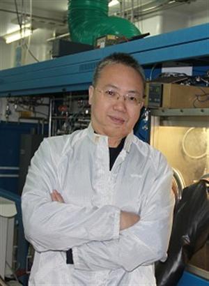
赵德刚,男,博士,研究员,博士生导师。
1972年出生。现任中科院半导体所光电子研究发展中心主任。2009年国家杰出青年科学基金获得者,2011年第十二届中国青年科技奖获得者,2018年国家中青年科技创新领军人才入选者,国家高层次人才,国家重点研发计划首席科学家,享受国务院政府特殊津贴专家。1994年、1997年在电子科技大学微电子科学与工程系分别获得学士和硕士学位,2000年在中国科学院半导体研究所获得博士学位。博士毕业后一直留所工作至今,主要从事GaN基光电子材料生长与器件研究,对材料生长机理、材料物理、器件设计及器件物理有较深入的理解和认识,解决了GaN材料大失配异质外延技术等关键难题,研制出我国第一支GaN基紫外激光器、长寿命大功率蓝光激光器和紫外雪崩光电探测器,还在碳杂质研究做出了系统性、创新性工作。主持和承担了国家重点研发计划、863、国家自然科学基金等多个项目,在Applied Physics Letters等著名学术刊物上发表SCI论文270多篇,获得国家发明专利30多项,撰写中文、英文专著各一章。
取得的主要学术成绩如下:
在GaN材料方面,我们深入研究了缓冲层原理,提出了独特的MOCVD外延方法,生长出高质量的GaN材料,室温下电子迁移率超过1000 cm2/Vs,这是目前国际上MOCVD外延的最好结果[D. G. Zhao et al, APL 89, 112106 (2006)];创造性提出了复合缓冲层结构,突破了无裂纹的AlN外延材料技术,其(002)、(102)面XRD半高宽均可控制在200弧秒;发现室温下GaN材料的应力状态主要取决于外延层和衬底之间的热失配,还发现GaN材料中的“黄光缺陷”和“蓝光缺陷”与刃位错和碳杂质紧密相关,并初步建立了GaN的光学、电学、结构性质的关系模型;发现了碳杂质对p-GaN材料的补偿效应,提出了少量掺氧的p型杂质激活方法,解决了p型掺杂难题。
在GaN器件方面,设计出能够监测紫外波长的新型器件,提出了利用紫外探测器的响应光谱对p-GaN载流子浓度进行测量的新方法;研究了p-GaN的欧姆接触工艺技术,实现了良好的欧姆接触特性,揭示了欧姆接触、空位缺陷和碳杂质对探测器的影响机理;研究了InGaN量子阱界面控制方法,分析了量子阱的电荧光光谱随注入电流变化的机制,并提出了相应的物理模型;提出了降低吸收损耗、抑制电子泄漏的多种激光器新结构,阐述了V型缺陷和碳杂质破坏发光器件性能的物理机制;研制出我国第一支GaN基紫外激光器、长寿命大功率蓝光激光器以及紫外雪崩光电探测器。
本人指导的研究生获得了中国科学院院长奖、国家奖学金、王守武奖学金、朱李月华优秀博士生奖等多种荣誉,本课题组拥有MOCVD设备及多种材料和器件测试分析仪器,实验条件较好,目前主要招收硕博连读生及博士生。
联系方式:
电话:010-82304208;Email: dgzhao@red.semi.ac.cn
在研/完成项目:
1、国家重点研发计划:“面向激光显示的三基色半导体激光器(LD)关键材料与技术基础研究”,2016.07-2020.12,主持
2、国家高层次人才计划:“GaN基光电子材料与器件”,2015.01-2017.12,主持
3、国家杰出青年科学基金:“GaN 基光电子材料与器件的基础问题”,2010.01-2013.12,主持
代表性学术论文(30篇):
F. Liang, D. G. Zhao*, D. S. Jiang, Z. S. Liu, J. J. Zhu, P. Chen, J. Yang, S. T. Liu, Y. Xing, and L. Q. Zhang, "Role of Si and C Impurities in Yellow and Blue Luminescence of Unintentionally and Si-Doped GaN", Nanomaterials 8, 1026 (2018) 【材料物理】
L. Y. Peng, D. G. Zhao*, D. S. Jiang, J. J. Zhu, Z. S. Liu, P. Chen, J. Yang, W. Liu, F. Liang, Y. Xing, S. T. Liu, L. Q. Zhang, W. J. Wang, M. Li, Y. T. Zhang, and G. T. Du, "Anomalous electroluminescent blue-shift behavior induced by well widths variance and localization effect in InGaN/GaN multi-quantum wells", Optics Express 26, 21736 (2018)【器件物理】
W. Liu, D. G. Zhao*, D. S. Jiang, D. P. Shi, J. J. Zhu, Z. S. Liu, P. Chen, J. Yang, F. Liang, S. T. Liu, Y. Xing, L. Q. Zhang, W. J. Wang, M. Li, Y. T. Zhang, and G. T. Du, "Effect of carrier transfer process between two kinds of localized potential traps on the spectral properties of InGaN/GaN multiple quantum wells", Optics Express, 26, 314174 (2018)【材料物理】
D. G. Zhao, J. Yang, Z. S. Liu, P. Chen, J. J. Zhu, D. S. Jiang, Y. S. Shi, H. Wang, L. H. Duan, L. Q. Zhang, and H. Yang, "Fabrication of room temperature continuous-wave operation GaN-based ultraviolet laser diodes", Journal of Semiconductors 38, 051001 (2017)【器件物理】
J. Yang, D. G. Zhao*, D. S. Jiang, P. Chen, J. J. Zhu, Z. S. Liu, W. Liu, X. Li, F. Liang, S. T. Liu, L. Q. Zhang and H. Yang, "Investigation on the corrosive effect of NH3 during InGaN/GaN multi-quantum well growth in light emitting diodes", Scientific Reports 7, 44850 (2017)【材料生长】
J. Yang, D. G. Zhao*, D. S. Jiang, P. Chen, Z. S. Liu, J. J. Zhu, X. J. Li, X. G. He, J. P. Liu, L. Q. Zhang, H. Yang, Y. T. Zhang, and G. T. Du, "Emission efficiency enhanced by reducing the concentration of residual carbon impurities in InGaN/GaN multiple quantum well light emitting diodes", Optics Express 24, 13824 (2016)【材料物理】
W. Liu, D. G. Zhao*, D. S. Jiang, P. Chen, Z. S. Liu, J. J. Zhu, X. Li, F. Liang, J. P. Liu, L. Q. Zhang, H. Yang, Y. T. Zhang, and G. T. Du, "Shockley–Read–Hall recombination and efficiency droop in InGaN/GaN multiple-quantum-well green light-emitting diodes", Journal of Physics D: Applied Physics 49, 145104 (2016)【器件物理】
W. Liu, D. G. Zhao*, D. S. Jiang, P. Chen, Z. S. Liu, J. J. Zhu, M. Shi, D. M. Zhao, X. Li, J. P. Liu, S. M. Zhang, H. Wang, H. Yang, Y. T. Zhang, and G. T. Du, "Temperature dependence of photoluminescence spectra for green light emission from InGaN/GaN multiple wells", Optics Express 23, 15935 (2015)【材料物理】
J. Yang, D. G. Zhao*, D. S. Jiang, P. Chen, J. J. Zhu, Z. S. Liu, L. C. Le, X. J. Li, X. G. He, J. P. Liu, H. Yang, Y. T. Zhang, and G. T. Du, "Optical and structural characteristics of high indium content InGaN/GaN multi-quantum wells with varying GaN cap layer thickness", Journal of Applied Physics 117, 055709 (2015)【材料生长】
J. Yang, D. G. Zhao*, D. S. Jiang, P. Chen, Z. S. Liu, L. C. Le, X. J. Li, X. G. He, J. P. Liu, S. M. Zhang, H. Wang, J. J. Zhu, and H. Yang, "Investigation on the compensation effect of residual carbon impurities in low temperature grown Mg doped GaN films", Journal of Applied Physics 115, 163704 (2014)【材料物理】
L. C. Le, D. G. Zhao*, D. S. Jiang, P. Chen, Z. S. Liu, J. Yang, X. G. He, X. J. Li, J. P. Liu, J. J. Zhu, S. M. Zhang, and H. Yang, "Suppression of electron leakage by inserting a thin undoped InGaN layer prior to electron blocking layer in InGaN-based blue-violet laser diodes", Optics Express 22, 11392 (2014)【器件设计】
L. C. Le, D. G. Zhao*, D. S. Jiang, L. Li, L. L. Wu, P. Chen, Z. S. Liu, J. Yang, X. J. Li, X. G. He, J. J. Zhu, H. Wang, S. M. Zhang, and H. Yang, "Effect of V-defects on the performance deterioration of InGaN/GaN multiple-quantum-well light-emitting diodes with varying barrier layer thickness", Journal of Applied Physics 114, 143706 (2013)【材料物理】
L. L. Wu, D. G. Zhao*, D. S. Jiang, P. Chen, L. C. Le, L. Li, Z. S. Liu, S. M. Zhang, J. J. Zhu, H. Wang, B. S. Zhang, and H. Yang, "Effects of thin heavily Mg-doped GaN capping layer on ohmic contact formation of p-type GaN", Semiconductor Science and Technology 28, 105020 (2013)【器件物理】
L. C. Le, D. G. Zhao*, D. S. Jiang, L. Li, L. L. Wu, P. Chen, Z. S. Liu, Z. C. Li, Y. M. Fan, J. J. Zhu, H. Wang, S. M. Zhang, and H. Yang, "Carriers capturing of V-defect and its effect on leakage current and electroluminescence in InGaN-based light-emitting diodes", Applied Physics Letters 101, 252110 (2012)【材料物理】
D. G. Zhao, D. S. Jiang, L. L. Wu, L. C. Le, L. Li, P. Chen, Z. S. Liu, J. J. Zhu, H. Wang, S. M. Zhang, and H. Yang, "Effect of dual buffer layer structure on the epitaxial growth of AlN on sapphire", Journal of Alloys and Compounds 544, 94 (2012)【材料生长】
D. G. Zhao, S. Zhang, D. S. Jiang, J. J. Zhu, Z. S. Liu, H. Wang, S. M. Zhang, B. S. Zhang, and H. Yang, "A study on the spectral response of back-illuminated p-i-n AlGaN heterojunction ultraviolet photodetector", Journal of Applied Physics 110, 053701 (2011)【器件物理】
D. G. Zhao, D. S. Jiang, J. J. Zhu, H. Wang, Z. S. Liu, S. M. Zhang, and H. Yang, " Hole concentration test of p-type GaN by analyzing the spectral response of p-n+ structure GaN ultraviolet photodetector ", Journal of Alloys and Compounds 492, 300 (2010)【器件物理】
D. G. Zhao, D. S. Jiang, J. J. Zhu, Z. S. Liu, H. Wang, S. M. Zhang, Y. T. Wang, and H. Yang, “Role of edge dislocation and Si impurity in linking the blue luminescence and yellow luminescence in n-type GaN films”,Applied Physics Letters 95, 041901 (2009)【材料物理】
D. G. Zhao, D. S. Jiang, J. J. Zhu, Z. S. Liu, S. M. Zhang and H. Yang, “A GaN photodetector integrated structure for wavelength characterization of ultraviolet light”,Semiconductor Science and Technology 23, 095021 (2008)【器件设计】
D. G. Zhao, D. S. Jiang, J. J. Zhu, Z. S. Liu, S. M. Zhang, H. Yang, U. Jahn, and K. H. Ploog, "Al composition variations in AlGaN films grown on low temperature GaN buffer layer by metalorganic chemical vapor deposition", Journal of Crystal Growth, 30, 5266 (2008)【材料生长】
D. G. Zhao, D. S. Jiang, J. J. Zhu, Z. S. Liu, S. M. Zhang, J. W. Liang, H. Yang, X. Li, X. Y. Li, and H. M. Gong, "Influence of defects in n—-GaN layer on the responsivity of Schottky barrier ultraviolet photodetectors", Applied Physics Letters 90, 062106 (2007)【器件物理】
D. G. Zhao, D. S. Jiang, J. J. Zhu, Z. S. Liu, S. M. Zhang, J. W. Liang and H. Yang, “Does an enhanced yellow luminescence imply a reduction of electron mobility in n-type GaN ?”, Journal of Applied Physics, 102, 113521 (2007)【材料物理】
D. G. Zhao, D. S. Jiang, J. J. Zhu, Z. S. Liu, S. M. Zhang, H. Yang, and J. W. Liang, , "Influence of V/III ratio in the initial growth stage on the properties of GaN epilayer deposited on low temperature AlN buffer layer", Journal of Crystal Growth, 303, 414 (2007)【材料生长】
D. G. Zhao, H. Yang, J. J. Zhu, D. S. Jiang, Z. S. Liu, S. M. Zhang, Y. T. Wang, and J. W. Liang, “Effects of edge dislocations and intentional Si doping on the electron mobility of n-type GaN films”, Applied Physics Letters 89, 112106 (2006)【材料生长】
D. G. Zhao, D. S. Jiang, H. Yang, J. J. Zhu, Z. S. Liu, S. M. Zhang, J. W. Liang, X. P. Hao, L. Wei, X. Liu, X. Y. Li, and H. M. Gong, “Effect of lightly Si doping on the minority carrier diffusion length in n-type GaN films ”, Applied Physics Letters 88, 252101 (2006)【器件物理】
D. G. Zhao, D. S. Jiang, H. Yang, J. J. Zhu, Z. S. Liu, S. M. Zhang, J. W. Liang, X. Liu, X. Y. Li, and H. M. Gong, “Role of edge dislocation in enhancing the yellow luminescence of n-type GaN ”, Applied Physics Letters, 88, 241917 (2006)【材料物理】
D. G. Zhao, J. J. Zhu, D. S. Jiang, H. Yang, J. W. Liang, X. Y. Li, and H. M. Gong, “Parasitic reaction and its effect on the growth rate of AlN by metalorganic chemical vapor deposition”, Journal of Crystal Growth, 289, 72 (2006)【材料生长】
D. G. Zhao, Z. S. Liu, J. J. Zhu, S. M. Zhang, D. S. Jiang, H. Yang, J. W. Liang, X. Y. Li, and H. M. Gong, “Effect of Al incorporation on the AlGaN growth by metalorganic chemical vapor deposition”, Applied Surface Science , 253, 2452 (2006)【材料生长】
D. G. Zhao, J. J. Zhu, Z. S. Liu, S. M. Zhang, H. Yang, D. S. Jiang, “Surface morphology of AlN buffer layer and its effect on the GaN growth by metalorganic vapor chemical deposition”, Applied Physics Letters 85, 1499 (2004)【材料生长】
D. G. Zhao, S. J. Xu, M. H. Xie, S. Y. Tong, and H. Yang, “Stress and its effect on optical properties of GaN epilayers grown on Si(111), 6H-SiC(0001), and c-plane sapphire”, Applied Physics Letters 83, 677 (2003)【材料物理】